- 您现在的位置:买卖IC网 > Sheet目录335 > ISL97635AIRZ (Intersil)IC LED DRVR WHT/RGB BCKLGT 24QFN
ISL97635A
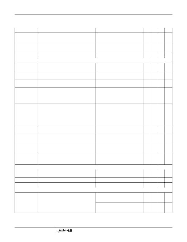
Electrical Specifications
All specifications below are tested at T A = -40°C to +85°C; V IN = 12V, EN = 5V, R SET = 36.6k Ω , unless
otherwise noted. Parameters with MIN and/or MAX limits are 100% tested at +25°C, unless otherwise
specified. Temperature limits established by characterization and are not production tested. (Continued)
PARAMETER
DESCRIPTION
CONDITION
MIN TYP MAX UNIT
t SU:DAT
t LOW
Data Setup Time
Clock Low Period
250
4.7
ns
μs
t HIGH
t F
t R
Clock High Period
Clock/Data Fall Time
Clock/Data Rise Time
4.0
50
300
1000
μs
ns
ns
GENERAL TIMING SPECIFICATIONS (Note 4)
t 1
Minimum Setup Time Between V IN Rising above
EN = 1, T A = +25°C, VDC capacitor < 10μF
80
μs
VUVLO with EN = 1 and SMBus Communications
t 2
Minimum Setup Time Between EN Going High with
V IN > VUVLO, T A = +25°C,
80
μs
V IN above VUVLO and SMBus Communications
VDC capacitor < 10μF
t 3
Minimum Time Between V IN Rising above VUVLO
EN = 1, T A = +25°C
4.5
ms
with EN = 1 to SMBus BL CTRL On
t 4
Minimum Time Between EN Going High with V IN
V IN > VUVLO, T A = +25°C
4.5
ms
above VUVLO to SMBus BL CTRL On
t 5
Minimum Time for LED Output to Respond to SMBus
V IN > VUVLO, EN = 1, T A = +25°C
5
μs
Data at any Levels
t 6
Response Time Between Backlight CTRL Off with
V IN > VUVLO, EN = 1, T A = +25°C
5
μs
Boost Not Switching to Backlight CTRL On with
Boost Switching
t 7
Response Time Between Backlight CTRL On with
V IN > VUVLO, EN = 1, T A = +25°C
5
μs
Boost Switching to Backlight CTRL Off with Boost
Not Switching
t 8
LED Channel Short Circuit Fault Detection to Status
V IN > VUVLO, EN = 1, T A = +25°C, LEDs
6
ms
Register Data Ready
Active
t 9
V OUT-GND Short Circuit Detection During Operation
V IN > VUVLO, EN = 1, T A = +25°C, Fault
5
μs
to Status Register Data Ready
FET used
t 10
Time Between VIN Rising Above VUVLO with
EN = 1, VDC capacitor < 10μF, T A = +25°C,
30
ms
EN = 1 and V OUT-GND Short being Reported in
Status Register
Fault FET used.
t 11
Time Between EN Going High with V IN Above
V IN > VUVLO, VDC capacitor < 10μF,
30
ms
VUVLO and a V OUT-GND Short being Reported in
Status Register
CURRENT SOURCES
T A = +25°C, Fault FET used.
V headroom
Dominant Channel Current Source Headroom at IIN
I LED = 20mA, T A = +25°C
100
mV
Pin
V RSET
I LEDmax
Voltage at RSET Pin
Maximum LED Current Per Channel
R SET = 36.6k Ω
R SET = 20.9k Ω
680
700
35
720
mV
mA
PWM GENERATOR (Note 4)
FPWM
DPWM
t MAX_PWM_OFF
Generated PWM Frequency
Duty Cycle of Generated PWM (DC-to-PWM)
Maximum PWMI Off-Time Before Shutdown
C FPWM = 27nF, C PWMO = 220nF
V PWMO = 0.3V CFPWM = 27nF
V PWMO = 1.1V CFPWM = 27nF
EN/PWMI toggles
200
90
10
28
Hz
%
%
ms
6
FN6564.2
December 22, 2008
发布紧急采购,3分钟左右您将得到回复。
相关PDF资料
ISL97635IRZ
IC LED DRVR WHT/RGB BCKLGT 24QFN
ISL97636AIRZ
IC LED DRIVR WHITE BCKLGT 24-QFN
ISL97636IRZ-TK
IC LED DRIVR WHITE BCKLGT 24-QFN
ISL97671AIRZ
IC LED DVR PWM CTRL 6CH 20QFN
ISL97672AIRZ
IC LED DRVR LOW DIMMING 20QFN
ISL97672BIRZ
IC LED DRVR BACKLIGHT 20QFN
ISL97675IRZ-TK
IC LED DVR PWM CTRL 4CH 20QFN
ISL97677IRZ
IC LED DVR PWM CTRL 8CH 32QFN
相关代理商/技术参数
ISL97635AIRZ-T
功能描述:IC LED DRVR WHT/RGB BCKLGT 24QFN RoHS:是 类别:集成电路 (IC) >> PMIC - LED 驱动器 系列:- 产品培训模块:Lead (SnPb) Finish for COTS
Obsolescence Mitigation Program 标准包装:2,500 系列:- 恒定电流:- 恒定电压:- 拓扑:升压(升压),切换式电容器(充电泵) 输出数:1 内部驱动器:是 类型 - 主要:背光 类型 - 次要:白色 LED 频率:625kHz ~ 875kHz 电源电压:2.7 V ~ 5.3 V 输出电压:5V 安装类型:表面贴装 封装/外壳:10-TFSOP,10-MSOP(0.118",3.00mm 宽) 供应商设备封装:10-µMAX 包装:带卷 (TR) 工作温度:-40°C ~ 85°C
ISL97635AIRZ-TK
功能描述:IC LED DRVR WHT/RGB BCKLGT 24QFN RoHS:是 类别:集成电路 (IC) >> PMIC - LED 驱动器 系列:- 产品培训模块:Lead (SnPb) Finish for COTS
Obsolescence Mitigation Program 标准包装:2,500 系列:- 恒定电流:- 恒定电压:- 拓扑:升压(升压),切换式电容器(充电泵) 输出数:1 内部驱动器:是 类型 - 主要:背光 类型 - 次要:白色 LED 频率:625kHz ~ 875kHz 电源电压:2.7 V ~ 5.3 V 输出电压:5V 安装类型:表面贴装 封装/外壳:10-TFSOP,10-MSOP(0.118",3.00mm 宽) 供应商设备封装:10-µMAX 包装:带卷 (TR) 工作温度:-40°C ~ 85°C
ISL97635AIRZ-TKR5306
制造商:Intersil Corporation 功能描述:
ISL97635IRZ
功能描述:IC LED DRVR WHT/RGB BCKLGT 24QFN RoHS:是 类别:集成电路 (IC) >> PMIC - LED 驱动器 系列:- 产品培训模块:Lead (SnPb) Finish for COTS
Obsolescence Mitigation Program 标准包装:2,500 系列:- 恒定电流:- 恒定电压:- 拓扑:升压(升压),切换式电容器(充电泵) 输出数:1 内部驱动器:是 类型 - 主要:背光 类型 - 次要:白色 LED 频率:625kHz ~ 875kHz 电源电压:2.7 V ~ 5.3 V 输出电压:5V 安装类型:表面贴装 封装/外壳:10-TFSOP,10-MSOP(0.118",3.00mm 宽) 供应商设备封装:10-µMAX 包装:带卷 (TR) 工作温度:-40°C ~ 85°C
ISL97635IRZ-T
功能描述:IC LED DRVR WHT/RGB BCKLGT 24QFN RoHS:是 类别:集成电路 (IC) >> PMIC - LED 驱动器 系列:- 产品培训模块:Lead (SnPb) Finish for COTS
Obsolescence Mitigation Program 标准包装:2,500 系列:- 恒定电流:- 恒定电压:- 拓扑:升压(升压),切换式电容器(充电泵) 输出数:1 内部驱动器:是 类型 - 主要:背光 类型 - 次要:白色 LED 频率:625kHz ~ 875kHz 电源电压:2.7 V ~ 5.3 V 输出电压:5V 安装类型:表面贴装 封装/外壳:10-TFSOP,10-MSOP(0.118",3.00mm 宽) 供应商设备封装:10-µMAX 包装:带卷 (TR) 工作温度:-40°C ~ 85°C
ISL97635IRZ-TK
功能描述:IC LED DRVR WHT/RGB BCKLGT 24QFN RoHS:是 类别:集成电路 (IC) >> PMIC - LED 驱动器 系列:- 产品培训模块:Lead (SnPb) Finish for COTS
Obsolescence Mitigation Program 标准包装:2,500 系列:- 恒定电流:- 恒定电压:- 拓扑:升压(升压),切换式电容器(充电泵) 输出数:1 内部驱动器:是 类型 - 主要:背光 类型 - 次要:白色 LED 频率:625kHz ~ 875kHz 电源电压:2.7 V ~ 5.3 V 输出电压:5V 安装类型:表面贴装 封装/外壳:10-TFSOP,10-MSOP(0.118",3.00mm 宽) 供应商设备封装:10-µMAX 包装:带卷 (TR) 工作温度:-40°C ~ 85°C
ISL97636AIRZ
功能描述:LED照明驱动器 6-CH LED DRVR RoHS:否 制造商:STMicroelectronics 输入电压:11.5 V to 23 V 工作频率: 最大电源电流:1.7 mA 输出电流: 最大工作温度: 安装风格:SMD/SMT 封装 / 箱体:SO-16N
ISL97636AIRZ-T
功能描述:IC LED DRIVR WHITE BCKLGT 24-QFN RoHS:是 类别:集成电路 (IC) >> PMIC - LED 驱动器 系列:- 产品培训模块:Lead (SnPb) Finish for COTS
Obsolescence Mitigation Program 标准包装:2,500 系列:- 恒定电流:- 恒定电压:- 拓扑:升压(升压),切换式电容器(充电泵) 输出数:1 内部驱动器:是 类型 - 主要:背光 类型 - 次要:白色 LED 频率:625kHz ~ 875kHz 电源电压:2.7 V ~ 5.3 V 输出电压:5V 安装类型:表面贴装 封装/外壳:10-TFSOP,10-MSOP(0.118",3.00mm 宽) 供应商设备封装:10-µMAX 包装:带卷 (TR) 工作温度:-40°C ~ 85°C
